
–
–
Events
–
–
Microfluidics Event
µTAS
Conference
Visit us at µTas to discover our high-precision solutions for microfluidics and life science applications. We will showcase customized microfluidic chips and components made of glass, quartz and silicon for applications such as lab-on-chip, diagnostics, droplet microfluidics, particle handling and optofluidics.
From precise microchannels, cavities and through-holes to optical windows and bonded assemblies, we support the development of microfluidic devices from prototype to series production. Discover the advantages of glass and quartz for demanding microfluidic applications. We look forward to meeting you in Granada!
Showcase products
> Microstructured components for life science applications
> Glass Microreactors and Micromixers

Meet PLANOPTIK at
Booth #38
Contact
Markus Schneider
+49 2664 5068 34
[email protected]
Website
Organizer
CBMS
[email protected]
Advanced Packaging Event
IMPACT-IAAC
Conference
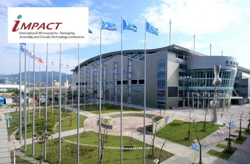
We are very happy to participate in the IMPACT IAAC Conference! Our team will be at the there to connect with industry experts and discuss the latest developments in advanced packaging. We are also excited to contribute to the technical program with a presentation highlighting our glass core substrates and glass wafers for wafer-level and panel-level packaging. We look forward to meeting you there!
Showcase products
> Glass Core Substrates for Advanced Packaging
> Wafers for Wafer-Level Packaging
> Carrier Wafers, Adapters & Tools
Date
October 19 – 22, 2026
Presentation date
Tuesday October 20th
Session S9 Glass substrate 13:00 – 15:00
701A, 7F, TaiNEX 2
Venue
Nangang International Exhibition Center, Hall 2, Taipei,
Taiwan
> Google Map
Presentation
Speaker
Jonas Discher
+49 2664 5068 21
[email protected]
Website
Organizer
IMPACT
[email protected]
Advanced Substrates & Semiconductor Solutions Event
Semicon Europa
Exhibition
We are excited to announce our participation in SEMICON Europa! At our booth, we will showcase our range of glass substrates for semiconductor manufacturing, including carrier wafers, adapters and tools, as well as glass wafers for the encapsulation of MEMS and sensors. We will also present wafers and panels for advanced packaging applications. We look forward to meeting industry experts and discussing innovative solutions and opportunities for collaboration.
Showcase products
> Carrier Wafers, Adapters and Tools
> Wafers for Wafer-Level-Packaging
> Glass Core Substrates for Advanced Packaging

Meet PLANOPTIK at
Hall B1, booth #912
Contact
Carsten Wesselkamp
+49 2664 5068 25
[email protected]
Website
Organizer
SEMI Europe
[email protected]
Advanced Substrates & Semiconductor Solutions Event
Semicon Japan
Exhibition
Join us at SEMICON Japan, one of the leading events for the semiconductor industry, bringing together the latest innovations in semiconductor manufacturing, equipment, materials, and technologies. We are looking forward to showcasing our high-quality glass wafers and discussing how our products support advanced semiconductor and precision manufacturing processes. Visit us and let’s shape the future of semiconductor manufacturing together!
Showcase products
> Carrier Wafers, Adapters and Tools
> Wafers for Wafer-Level Packaging
> Glass Core Substrates for Advanced Packaging

Meet PLANOPTIK at
Booth number to follow
Contact
Carsten Wesselkamp
+49 2664 5068 25
[email protected]
Website
Organizer
SEMI Japan
[email protected]
Microfluidics Event
SLAS 2027
Conference & Exhibition
…Event details to follow…
Showcase products
> Components for life science
> Microsystems for flow chemistry

Meet PLANOPTIK at
Booth #553
Contact
Alexander Schilling
+49 2664 5068 34
[email protected]
Website
Organizer
Society for Laboratory Automation and Screening
Advanced Glass Substrates Event
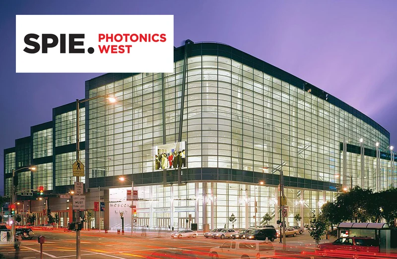
SPIE Photonics West
Exhibition
…Event details to follow…
Showcase products
> Glass Wafers, Quartz Wafers & Silicon Wafers
> Carrier Wafers, Adapters & Tools
> Glass Core Substrates for Advanced Packaging
Meet PLANOPTIK at
Booth number to follow
Contact
Jonas Discher
+49 2664 5068 21
[email protected]
Website
Organizer
SPIE
Semiconductor solutions Event
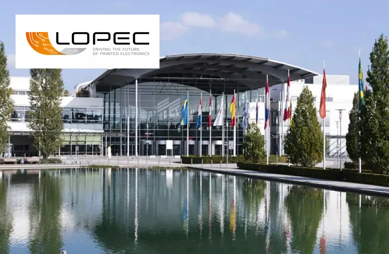
LOPEC
Exhibition
…Event details to follow…
Showcase products
> Carrier Wafers, Adapters & Tools
> Glass Wafers, Quartz Wafers & Silicon Wafers
Meet PLANOPTIK at
Booth number to follow
Contact
Carsten Wesselkamp
+49 2664 5068 25
[email protected]
Website
Organizer
Munich Trade Fair Centre
Microfluidics Event
Flow Chemistry Europe
Conference & Exhibition
…Event details to follow…
Showcase products
> Microsystems for flow chemistry
> Components for life science

Date
April 14 – 16, 2027
Venue
Malaga, Spain
Meet PLANOPTIK at
Booth number to follow
Contact
Alexander Schilling
+49 2664 5068 34
[email protected]
Website
Organizer
Flow Chemistry Society
Advanced Packaging Event
IEEE – ECTC
Conference & Exhibition
…Event details to follow…
Showcase products
> Glass Core Substrates for Advanced Packaging
> Glass Wafers, Quartz Wafers & Silicon Wafers

Meet PLANOPTIK at
Booth number to follow
Contact
Jonas Discher
+49 2664 5068 21
[email protected]
Website
Organizer
IEEE
Microfluidics Event
Achema
Exhibition
…Event details to follow…
Showcase products
> Microsystems for flow chemistry
> Components for life science

Meet PLANOPTIK at
Booth number to follow
Contact
Alexander Schilling
+49 2664 5068 34
[email protected]
Website
Organizer
Dechema
Semiconductor solutions event
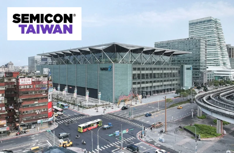
Semicon Taiwan
Exhibition
…Event details to follow…
Showcase products
> Carrier Wafers, Adapters & Tools
> Glass Wafers, Quartz Wafers & Silicon Wafers
Meet PLANOPTIK at
Booth number to follow
Contact
Carsten Wesselkamp
+49 2664 5068 25
[email protected]
Website
Organizer
SEMI Taiwan
[email protected]
–
–
Team up with PLANOPTIK
–
–

–
–
Individually developed
Are you developing a new microsystem? Are you combining microelectronics, micromechanics or microfluidics to create a new product? Are you developing a sensor, an electronic device, a fluidic system or something that has never existed before? Team up with PLANOPTIK.
–
–
Reliable partnership
In us you will find a partner who will work with you to develop electronic, mechanical, optical, chemical or biological microcomponents and has a firm grasp of materials such as glass, silicon and copper.
–
–
Together until production
PLANOPTIK also manufactures the jointly developed microcomponents and elements in high volumes using state-of-the-art wafer-based manufacturing processes.