
–
–
Technologies
–
–
–
–
Technologies for functional glass wafers and microsystems
PLANOPTIK combines a broad range of wafer- and panel-level technologies for the development and series production of high-precision glass-based components.
Our capabilities go far beyond the manufacture of precision substrates. We structure glass, create electrical and functional layers, combine different materials by bonding and integrate multiple process steps into complete manufacturing sequences.
This allows us to turn glass, quartz and silicon substrates into functional components for semiconductor packaging, MEMS, microfluidics and other microsystem applications.
–
–
Independent material selection
–
–
PLANOPTIK is independent of the major glass manufacturers. This allows us to select the material that best meets the technical requirements of each individual application, without being tied to a specific manufacturer or material portfolio.
Depending on the application, we process technical and optical glasses, high-purity fused silica and other suitable materials from leading manufacturers in the USA, Europe and Asia.
In addition, we keep a broad range of commonly used materials in stock, in some cases in significant quantities. This allows us to start production quickly and reduces lead times for many standard materials.
Our material independence, combined with a well-stocked material inventory, enables us to select the most suitable material for each application while maintaining a high degree of flexibility and short response times.
–
–
Micro structuring & patterning
–
–
–
–
Creating functional structures in glass
Micro structuring is one of PLANOPTIK’s key technologies. Depending on feature size, geometry, depth, sidewall profile and surface requirements, we use different structuring processes and select the technology best suited to the respective application.
Our capabilities include:
– CHEMICAL(WET) ETCHING
– LASER PROCESSING
– SELECTIVE LASER INDUCED ETCHING (SLE)
– DEEP REACTIVE ION ETCHING
– SANDBLASTING
Typical structures include:
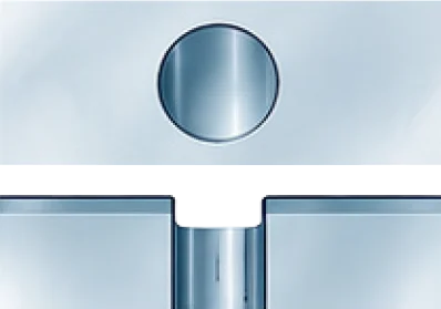
Through-Glass VIAS
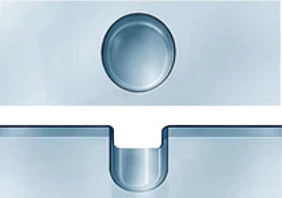
Blind holes
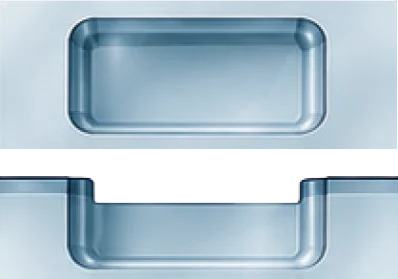
Cavities
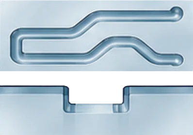
Channels
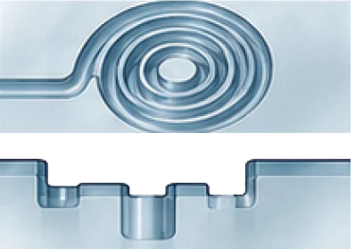
Microfluidic structures
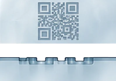
Markings
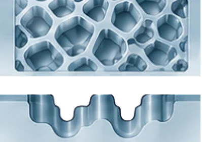
Customer-specific Patterns
–
–
Shaping
–
–
–
–
Transforming glass into wafers and panels
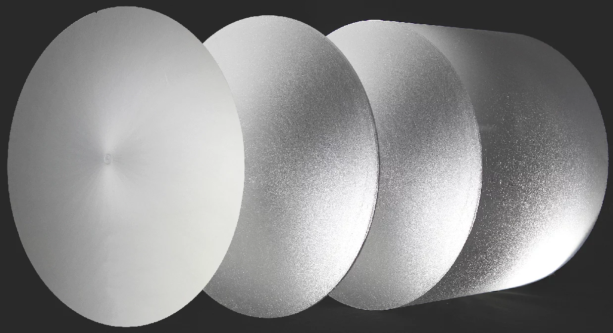
The production of wafers and panels begins with the raw material. Using precise processes, the material is cut into wafers or panels with various geometries. These processes include for example:
– DIAMOND CUTTING
– WATER-JET CUTTING
– WIRE SAWING
– EDGE GRINDING
–
–
Surface Treatment and Finishing
–
–
–
–
From substrates to products with high-precision surfaces
Next, various steps are taken to achieve the quality and dimensional accuracy specified by the customer. Therefore, the following processes could be used:
– GRINDING
– POLISHING
– Regular Polishing
– MDF polishing
Our processes enable us to achieve high quality surfaces with
- Thickness down to 200 μm
- TTV from 1 µm (depending on wafer thickness and diameter)
- Surface roughness down ≤ 0.5 nm (Ra)
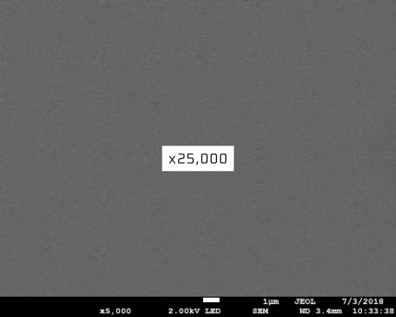
Our MDF polishing process allows a clean etching process
–
–
Further Processing
–
–
–
–
Enabling functionality through advanced process steps
Following the structuring process, additional manufacturing steps are often required to transform the substrate into a fully functional component. Depending on the application, these processes may include metallization for electrical conductivity, coating to enhance optical, mechanical, or chemical properties, bonding for the integration of multiple materials or components, and dicing for the separation of individual devices.
The selection and combination of these processes are tailored to the specific product requirements, ensuring optimal functionality, reliability, and performance in demanding high-tech applications.
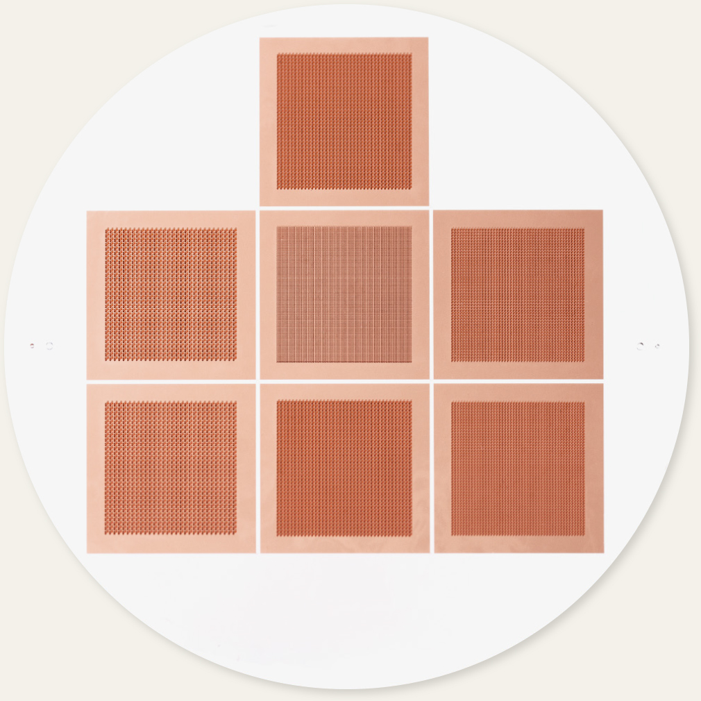
Metallisation
Full-Surface copper metallization
by cu-liner strategy
- Substrate material: Borofloat33, quartz
- Wafer Diameter: up to 300 mm
- Panel Dimension: up to 300 x 300 mm
- Panel Dimension: up to 300 x 300 mm
- Substrate thickness: 300 – 1000 μm
- Hole diameter: ≥75 μm
- Pitch: twice hole diameter
- Cu thickness: 2..10 μm
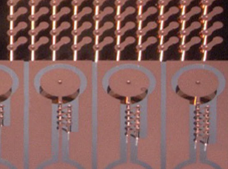
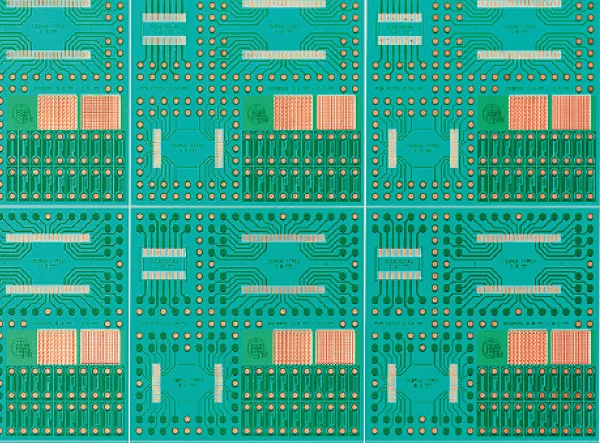
Redistribution layer
- Customized RDL up to 200 mm diameter
- Line / Space: 50 µm / 50 µm
Lithography
- Dry resist
- Solder Mask
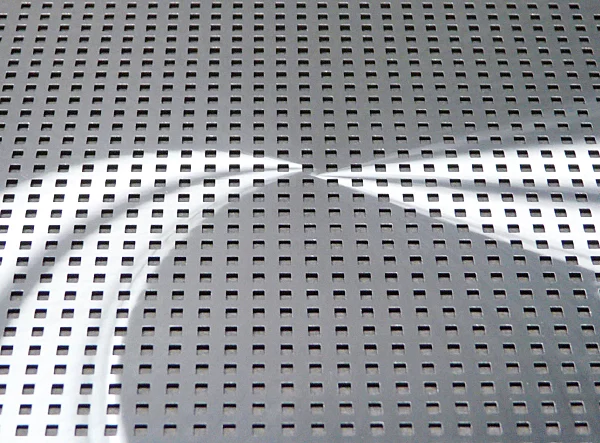
Various Coatings
- ITO
- Titanium
- Copper
- Alu
- Chrome
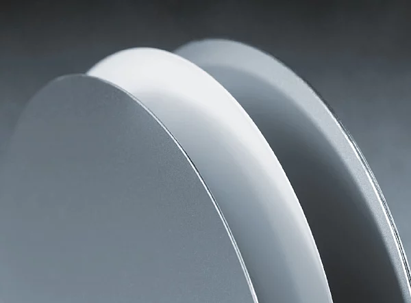
Bonding
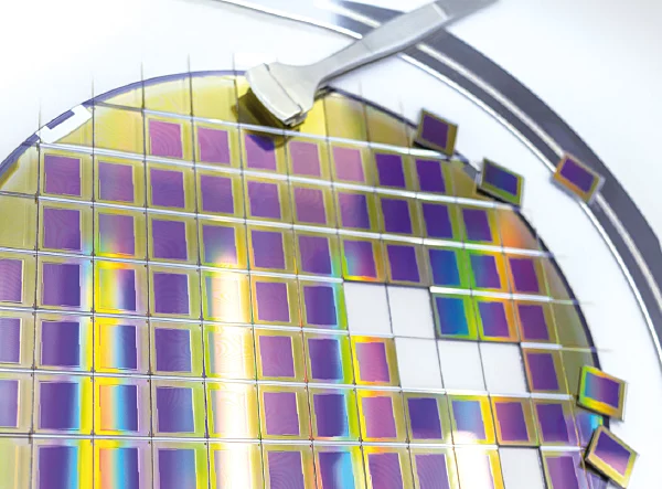
Dicing
Lithography
- Dry resist
- Solder Mask
Various Coatings
- ITO
- Titanium
- Copper
- Alu
- Chrome
–
–
Team up with PLANOPTIK
–
–

–
–
Individually developed
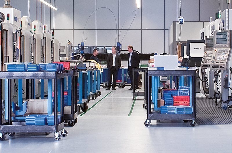
Are you developing a new microsystem? Are you combining microelectronics, micromechanics or microfluidics to create a new product? Are you developing a sensor, an electronic device, a fluidic system or something that has never existed before? Team up with PLANOPTIK.
–
–
Reliable partnership
In us you will find a partner who will work with you to develop electronic, mechanical, optical, chemical or biological microcomponents and has a firm grasp of materials such as glass, silicon and copper.
–
–
Together until production
PLANOPTIK also manufactures the jointly developed microcomponents and elements in high volumes using state-of-the-art wafer-based manufacturing processes.