
–
–
ABOUT PLANOPTIK
–
–
–
–
Let’s talk about glass
–
–
Glass is the foundation of our expertise.
PLANOPTIK develops and manufactures high-precision glass wafers, substrates and micro components for advanced applications in the semiconductor industry, microsystems technology and microfluidics.
Our highly specialized products help enable next-generation sensors, advanced semiconductor packaging, miniaturized electronic devices and innovative solutions for medical, pharmaceutical and chemical applications.
By combining the unique properties of glass with advanced wafer-level manufacturing technologies, we create solutions precisely tailored to our customers’ applications.


–
–
Precision beyond the ordinary
–
–
Our roots lie in precision optics – and precision still defines everything we do.
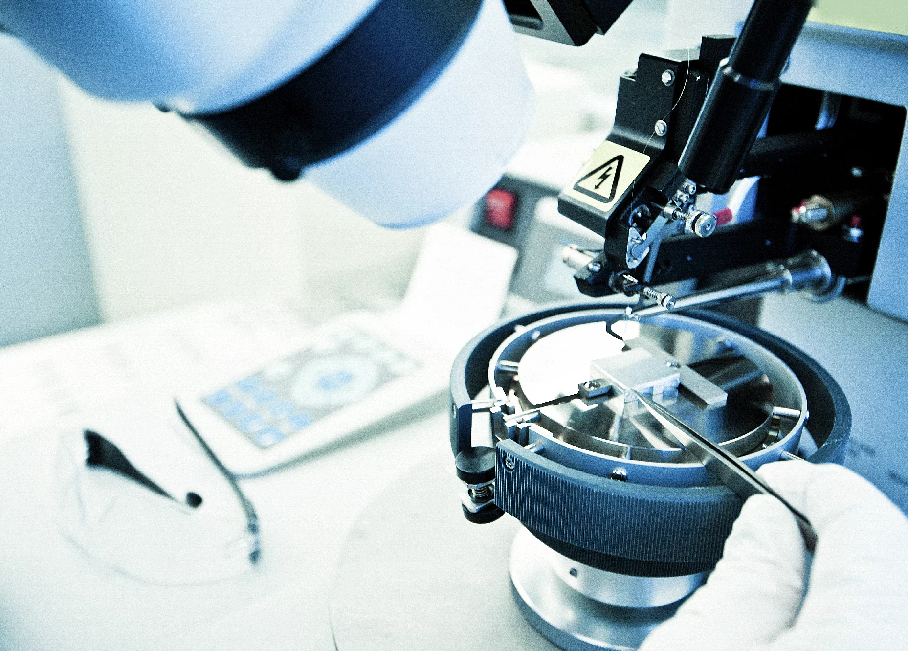
PLANOPTIK processes glass, quartz, silicon and material combinations with extremely tight dimensional tolerances and surface roughness down to the sub-nanometer range.
Using technologies such as precision polishing, micro structuring, laser processing, chemical etching, coating, metallization, bonding and dicing – complemented by proprietary and internally optimized processes such as MDF polishing – we transform wafers and panels into functional components for demanding high-tech applications.
From simple high-precision substrates to complex micro structured components, every product is developed and manufactured according to the specific requirements of its application.
–
–
From development to series production
–
–
Our customers are our partners.
We often become involved at an early stage of product development, working closely with our customers to turn an initial idea or specification into a manufacturable solution. Our expertise covers materials, design for manufacturing, micro structuring and the integration of mechanical, optical, electrical, chemical and fluidic functions.
But our role does not end with development. Once a solution has been qualified, PLANOPTIK can manufacture it reliably in series using wafer- and panel-based production processes. Many of these partnerships continue for years as we supply components directly into our customers’ production processes.
Our manufacturing infrastructure includes approximately 300 m² of cleanroom production area for selected wafer-level processes requiring controlled particle conditions. Today, more than 100 employees support customers and partners in more than 40 countries.

–
–
Global reach. Industrial scale.
–
–
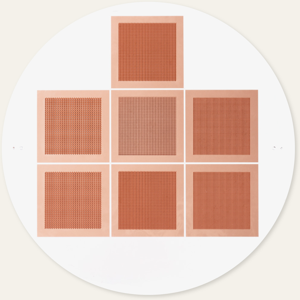
PLANOPTIK is one of the world’s leading suppliers of high-precision glass wafers, substrates and microcomponents for advanced technology applications.
Every year, we supply more than 500,000 wafers and millions of finished components to customers and partners worldwide. This scale combines specialized glass expertise with the process stability, manufacturing capacity and reliability required for international series production.
From initial development quantities to long-term high-volume supply, customers in more than 40 countries rely on PLANOPTIK as an established partner for critical components
–
–
Independent in material selection
–
–
PLANOPTIK is independent of the major glass manufacturers. This gives us the freedom to select the material that is best suited to each individual application, rather than being limited to a specific supplier or material portfolio.
Depending on the requirements, we work with technical and optical glasses, high-purity fused silica and other suitable materials from leading manufacturers in the USA, Europe and Asia. For our customers, this means that material selection is driven by the application – not by supplier dependency.


–
–
Innovation starts with the right material
–
–
Many new products require components that go beyond conventional solutions.
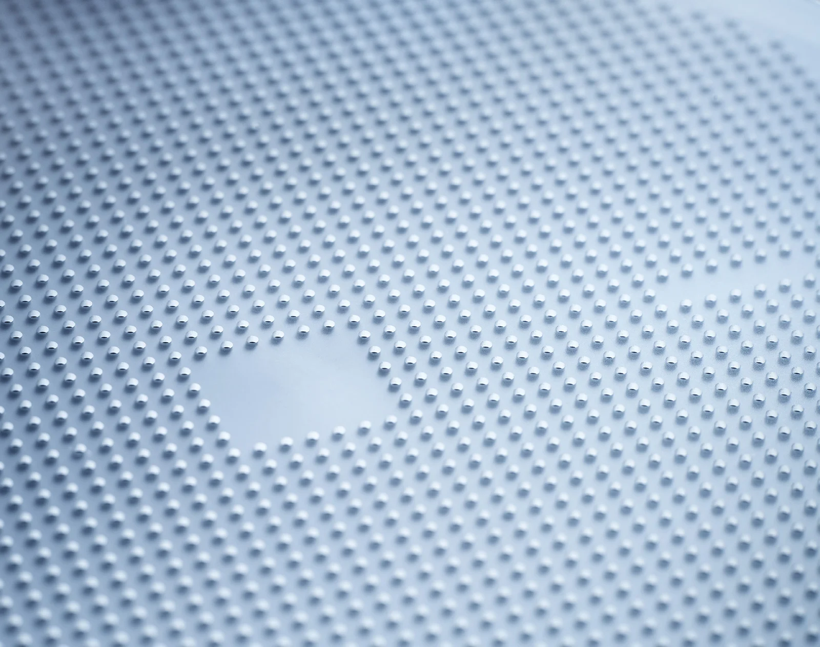
Glass offers a unique combination of dimensional stability, chemical resistance, electrical insulation, optical transparency and compatibility with semiconductor manufacturing processes. PLANOPTIK combines these properties with advanced micro structuring and processing technologies to create components that add new functions to our customers’ products.
Whether you are developing a new sensor, an advanced packaging solution, a microfluidic device or an entirely new microsystem, we help turn your requirements into a manufacturable component.
–
–
Every nanometer counts
–
–
In microsystems technology, small differences can have a major impact.
Surface quality, thickness variation, dimensional accuracy and microstructure geometry can determine whether a component performs as intended.
That is why precision at PLANOPTIK goes beyond dimensional tolerances alone. We combine high-precision manufacturing technologies with extensive process expertise to achieve consistent and reproducible results – from prototypes to high-volume production.
–
–
Certified quality and environmental responsibility
–
–
Quality and reliability are essential when components become part of our customers’ products and production processes.
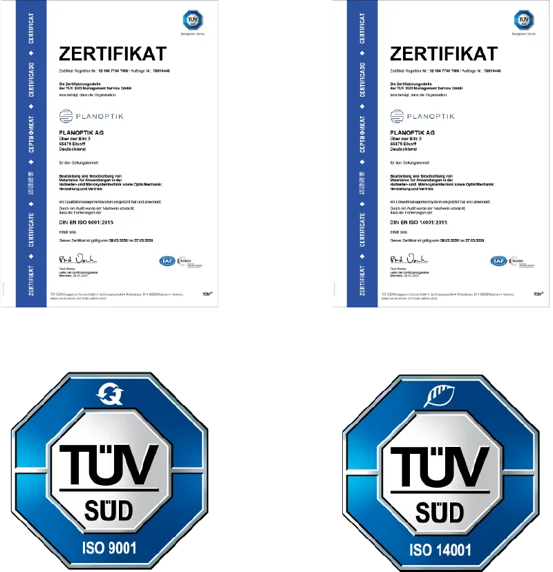
PLANOPTIK AG operates a quality management system certified according to ISO 9001. Our processes are designed to ensure consistent product quality from incoming materials through manufacturing and inspection to final packaging and shipment.
Our environmental management system is certified according to ISO 14001. We continuously work to reduce the environmental impact of our operations and to use energy, materials and resources responsibly.
–
–
Careers at PLANOPTIK
–
–
Shape the technologies of tomorrow
PLANOPTIK is an internationally active high-tech company combining the agility of a medium-sized business with the technological challenges of global semiconductor, microsystems and life-science markets.
Our employees work on products and technologies that often cannot simply be bought off the shelf – they have to be developed. If you enjoy solving technical challenges, taking responsibility and working on products that will become part of tomorrow’s technologies, we would like to hear from you.
–
–
Team up with PLANOPTIK
–
–

–
–
Individually developed
Are you developing a new microsystem? Are you combining microelectronics, micromechanics or microfluidics to create a new product? Are you developing a sensor, an electronic device, a fluidic system or something that has never existed before? Team up with PLANOPTIK.
–
–
Reliable partnership
In us you will find a partner who will work with you to develop electronic, mechanical, optical, chemical or biological microcomponents and has a firm grasp of materials such as glass, silicon and copper.
–
–
Together until production
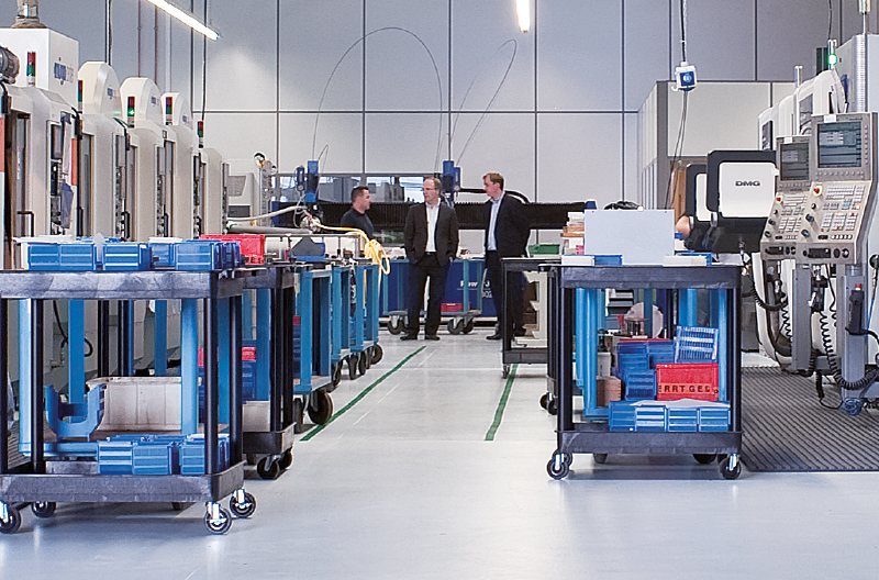
PLANOPTIK also manufactures the jointly developed microcomponents and elements in high volumes using state-of-the-art wafer-based manufacturing processes.