
–
–
Glass Core Substrates
–
–
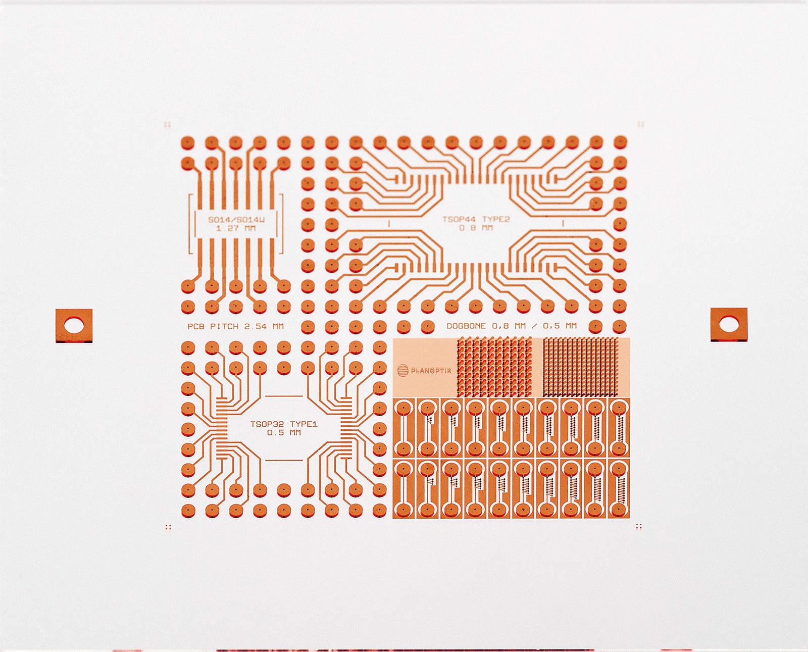
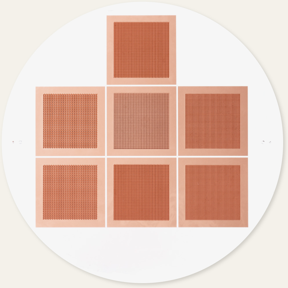
PLANOPTIK develops Glass Core Substrates for advanced packaging, providing a high-precision platform for attaching and interconnecting microchips and semiconductor components.
The glass core is processed with fine through-glass vias and copper metallization, enabling reliable routing and high-density electrical interfaces using wafer-level manufacturing and lithographic structuring.
–
–
Glass Core Substrates enable chips and sensors to be stacked in the smallest of spaces.
Individually developed.
–
–
Discover the technologies we offer to shape Glass Core Substrates for Advanced Packaging. Individually developed and manufactured from R&D to high volumes.
– THROUGH-GLASS-VIAS
– METALLIZIATION
– CAVITIES
– DIFFERENT GLASS TYPES
– MDF POLISHING
– MARKINGS
– DICING
– REDISTRIBUTION LAYER (RDL)
– SOLDER MASK
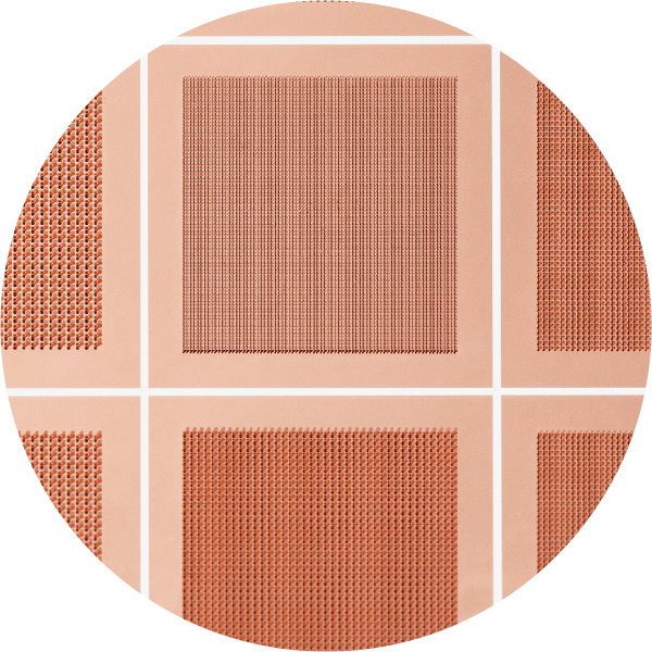
Metallisation

Through Glass VIAS
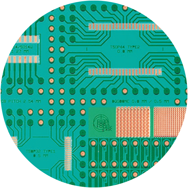
Solder mask

Redistribution layer

MDF Polishing
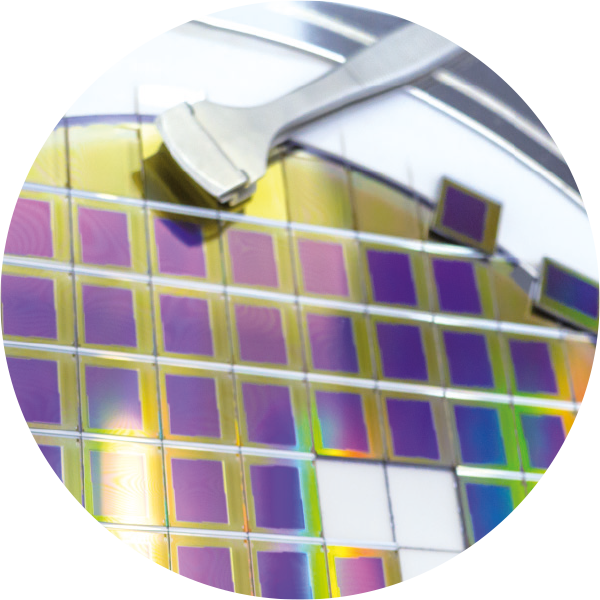
Dicing
–
–
Glass – the best choice
for Advanced Packaging
Glass – the best choice for Advanced Packaging
Glass is becoming a key material for advanced packaging and high-density interconnects. Compared to conventional organic PCB substrates, glass offers outstanding dimensional stability, electrical insulation and thermal reliability – enabling tighter layouts and more robust packages.
Key advantages of glass vs. classic PCBs:
- Higher dimensional stability for fine-pitch routing and accurate alignment
- Excellent electrical insulation with low signal losses at high frequencies
- Low CTE and high thermal stability for reduced warpage and improved reliability
- High stiffness and flatness for advanced assembly and multi-chip integration
- High-precision through-glass vias (TGVs) for vertical interconnects and dense I/O
These properties make Glass Core Substrates an ideal platform for next-generation semiconductor packaging, especially for high-performance computing and RF applications.
–
–
3D Packaging based on
Glass Core Substrates
3D Packaging based on Glass Core Substrates
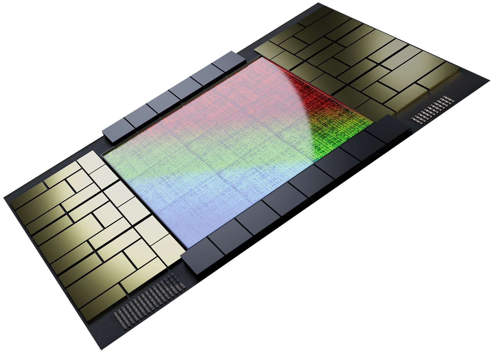
Glass Core Substrates are used in advanced packaging to connect and integrate multiple chips and electronic components in one compact module. Acting as a high-precision interconnect platform, they enable dense routing and reliable signal transmission – especially when space is limited and performance requirements are high.
This makes Glass Core Substrates ideal for next-generation electronics such as AI hardware, high-speed data communication, and RF applications, where smaller, faster and more energy-efficient devices are required.
–
–
Interposers
and structured
Glass Core Substrates
–
–
A key application for Glass Core Substrates is interposers. Interposers act as high-density routing layers that connect multiple chips within one package, enabling compact multi-chip modules and 2.5D integration. PLANOPTIK manufactures glass interposers using wafer-based processes.
–
–
How to create a Glass Core Substrate

Glass wafer with micro holes, copper coated

Wafer additionally coated with solder resist

Interposer after dicing
–
–
Meet with PLANOPTIK
–
–
Advanced Substrates & Semiconductor Solutions Event
Semicon Europa
Exhibition
We are excited to announce our participation in SEMICON Europa! At our booth, we will showcase our range of glass substrates for semiconductor manufacturing, including carrier wafers, adapters and tools, as well as glass wafers for the encapsulation of MEMS and sensors. We will also present wafers and panels for advanced packaging applications. We look forward to meeting industry experts and discussing innovative solutions and opportunities for collaboration.
Showcase products
> Carrier Wafers, Adapters and Tools
> Wafers for Wafer-Level-Packaging
> Glass Core Substrates for Advanced Packaging

Meet PLANOPTIK at
Hall B1, booth #912
Contact
Carsten Wesselkamp
+49 2664 5068 25
[email protected]
Website
Organizer
SEMI Europe
[email protected]
Advanced Substrates & Semiconductor Solutions Event
Semicon Japan
Exhibition
Join us at SEMICON Japan, one of the leading events for the semiconductor industry, bringing together the latest innovations in semiconductor manufacturing, equipment, materials, and technologies. We are looking forward to showcasing our high-quality glass wafers and discussing how our products support advanced semiconductor and precision manufacturing processes. Visit us and let’s shape the future of semiconductor manufacturing together!
Showcase products
> Carrier Wafers, Adapters and Tools
> Wafers for Wafer-Level Packaging
> Glass Core Substrates for Advanced Packaging

Meet PLANOPTIK at
Booth #E7984
Contact
Carsten Wesselkamp
+49 2664 5068 25
[email protected]
Website
Organizer
SEMI Japan
[email protected]
Advanced Glass Substrates Event
SPIE Photonics West
Exhibition
Visit us at SPIE Photonics West in San Francisco! At Photonics West we will showcase our wide range glass subs for photonics, optoelectronics, MOEMS-MEMS, and biomedical optics. From excellent optical transparency to precision microstructuring, including through-holes and cavities, as well as wafer bonding, our solutions support your projects from prototype to series production. Visit us at the Moscone Center and discover how our wafers can advance your next photonics project.
Showcase products
> Glass Wafers, Quartz Wafers & Silicon Wafers
> Carrier Wafers, Adapters & Tools
> Glass Core Substrates for Advanced Packaging

Meet PLANOPTIK at
Booth #4246
Contact
Jonas Discher
+49 2664 5068 21
[email protected]
Website
Organizer
SPIE
Advanced Packaging Event
IEEE – ECTC
Conference & Exhibition
…Event details to follow…
Showcase products
> Glass Core Substrates for Advanced Packaging
> Glass Wafers, Quartz Wafers & Silicon Wafers

Meet PLANOPTIK at
Booth number to follow
Contact
Jonas Discher
+49 2664 5068 21
[email protected]
Website
Organizer
IEEE

–
–
Team up with PLANOPTIK
–
–

–
–
Individually developed
Are you developing a new microsystem? Are you combining microelectronics, micromechanics or microfluidics to create a new product? Are you developing a sensor, an electronic device, a fluidic system or something that has never existed before? Team up with PLANOPTIK.
–
–
Reliable partnership
In us you will find a partner who will work with you to develop electronic, mechanical, optical, chemical or biological microcomponents and has a firm grasp of materials such as glass, silicon and copper.
–
–
Together until production
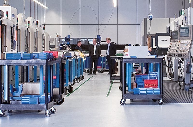
PLANOPTIK also manufactures the jointly developed microcomponents and elements in high volumes using state-of-the-art wafer-based manufacturing processes.